
FALIT®
ICO Laser - Decap EMC
Using precise energy control, the focus of ICOTM Laser can remove the epoxy mold compound, while leaving the bonding wire and the lead frame undamaged.
FAQ
How can you control the laser energy from burning the bond wire?
CLC developed APEX laser motion control card, which precisely controls the laser pulse energy and beam motion to ensure the spot energy density does not damage the bond wire.
GEL Laser - Decap Clear Packages
The GELTM Laser beam focus evaporates the silica gel using the GEL-BLUETM solution as a solvent on the last layer above the die, guaranteed non-destructive.
FAQ
Why are we unable to use the ICO laser to do gel removal?
Because the photon energy emitted from ICO laser does not have a good absorption rate when applied to silica gel, Our Gel laser has the proper absorption rated to remove GEL material.
Xsec Laser - Cross Section
The XSECTM Laser emits high peak power pulsed photons that evaporate the desired cross section line with a narrow kerf width.
FAQ
Why do we need the XSEC laser to do the cross section?
Because the XSEC ultrafast laser emits pulses at a picosecond width to gain the zero heat effect zone and yield a clean cut edge.
Xsec Laser - Delidding
The XSECTM Laser emits high peak power pulsed photons that ablate the required material for de-lidding, guarantying non-contamination inside the device.
FAQ
Can we de-lidding the ceramic IC packages?
Yes, the XSEC laser can de-lidding the KOVAR, aluminum alloy and all types of ceramic IC packages. along with PCB material, of course.
ECO Laser - Nondestructive Photochemcial Decap
The ECOTM Laser emits short wavelength photons, at the same time using an ultrafast scan in conjunction with the CLC proprietary ECO BLUETM solvent. The results are a non-destructive decap to the die without the aid of acid.
FAQ
How can the high energy laser guarantee non-destructive results? Does this process fit all type of dies?
The ECO laser ultrafast scan using the photochemical solvent, activates and destroys the cross link of EMC. The solvent is the key role to do the decap process. The process is fit for all types of dies, including Si, Ge, GaAs, SiC etc.
Delayering Laser - Inspecting TSV
The DeLayeringTM Laser emits an ultrafast, short wavelength of photons to remove the RDL, layer by layer, to inspect TSV defects in the advanced IC packaging.
FAQ
Can we remove the RDL layer without damage the underneath layer?
Yes, by controlling the laser focal depth to be less than the isolation layer thickness. The process works with the PicoeyeTM 5 micron video microscope. The use of the Picoeye during the process success guarantees measurable results.
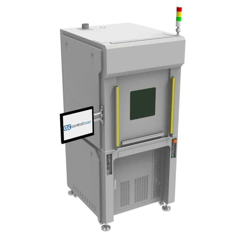
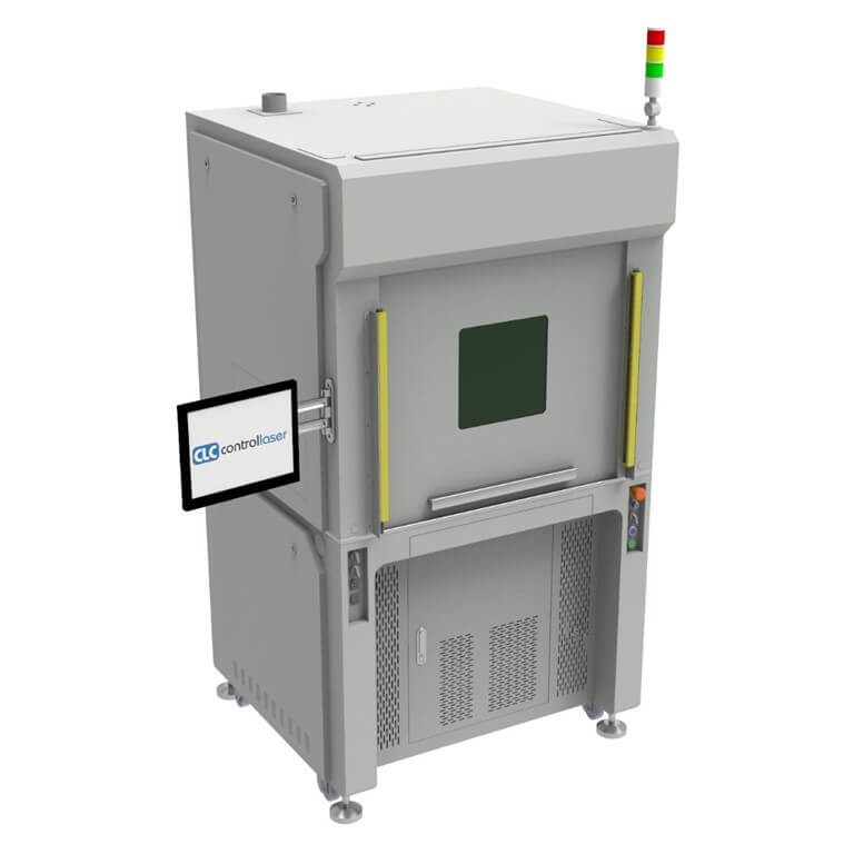
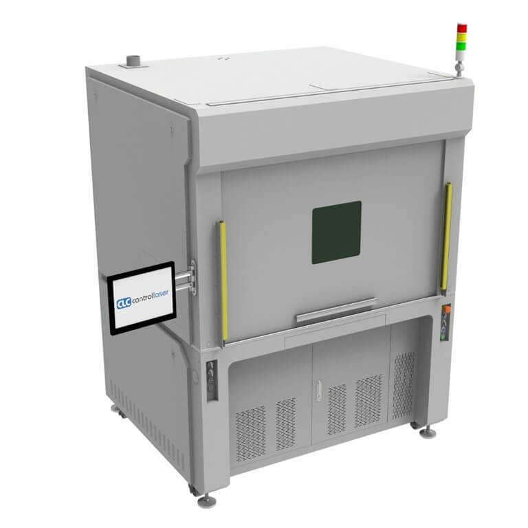
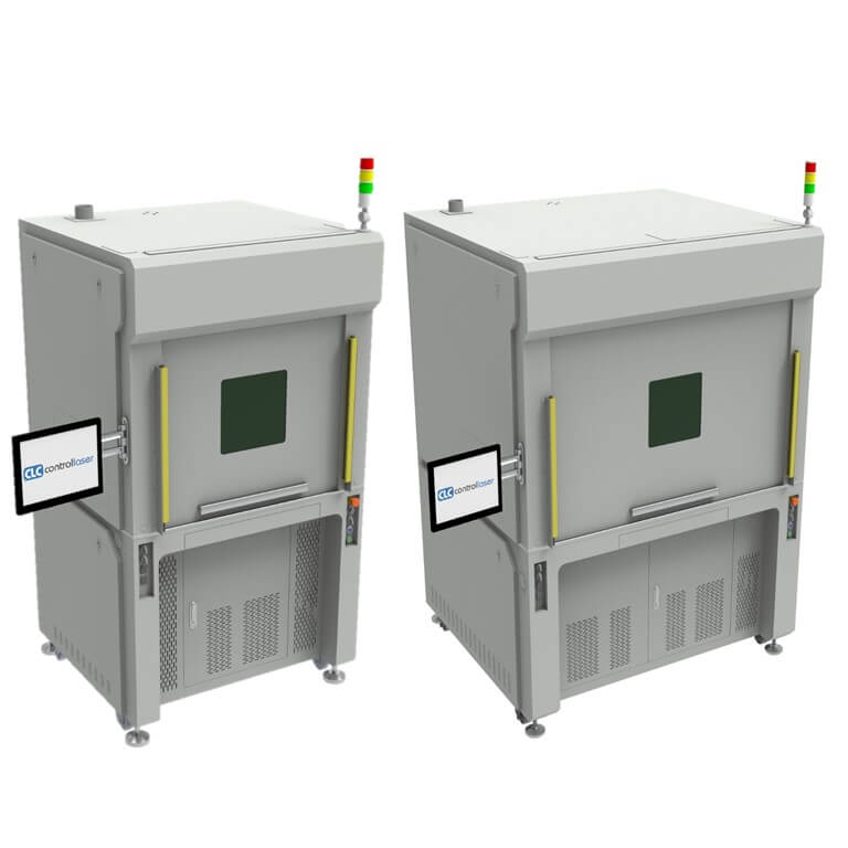
Build Your Own 1/3
Select Laser(s) by Application:
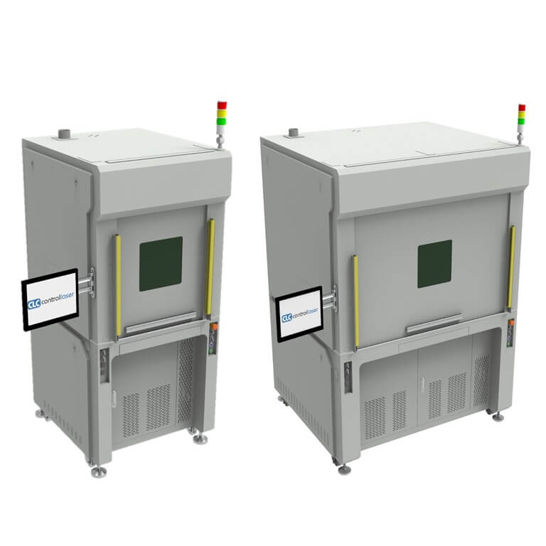
Build Your Own 2/3
Click to Select Workstation by Laser Quantity

Build Your Own 3/3
Click to Select Video Mircoscopes by Applied IC Size
Notes: Select the proper video microscope based your target IC size, use IR Thermal Imaging to quickly locate the defect spots.
Custom engineering services are available upon request for microscope lenses with Field of View (FoV) ranging from 1 micron to 100 mm.
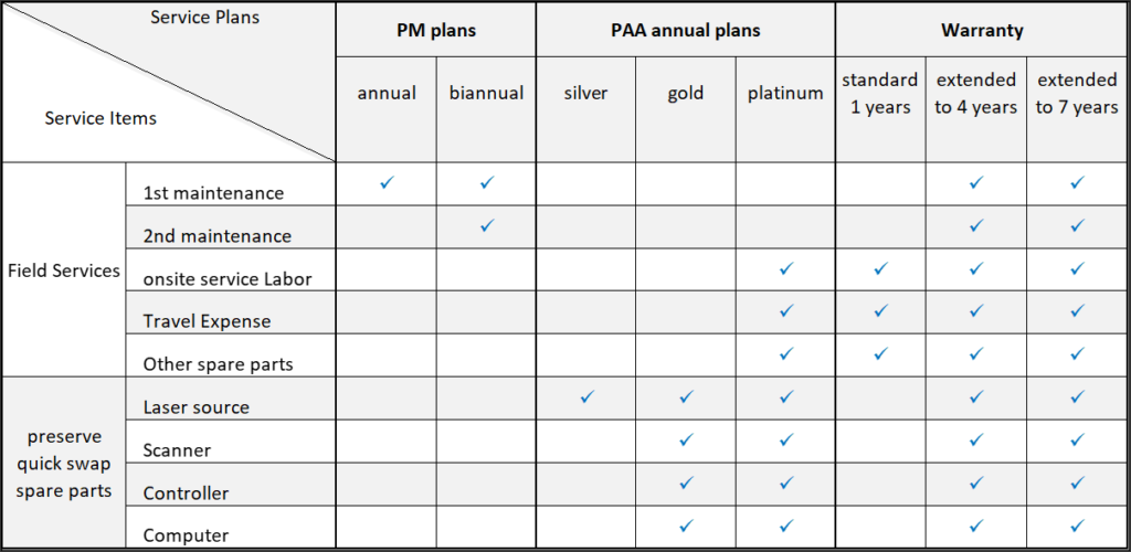
Options: Service Plans
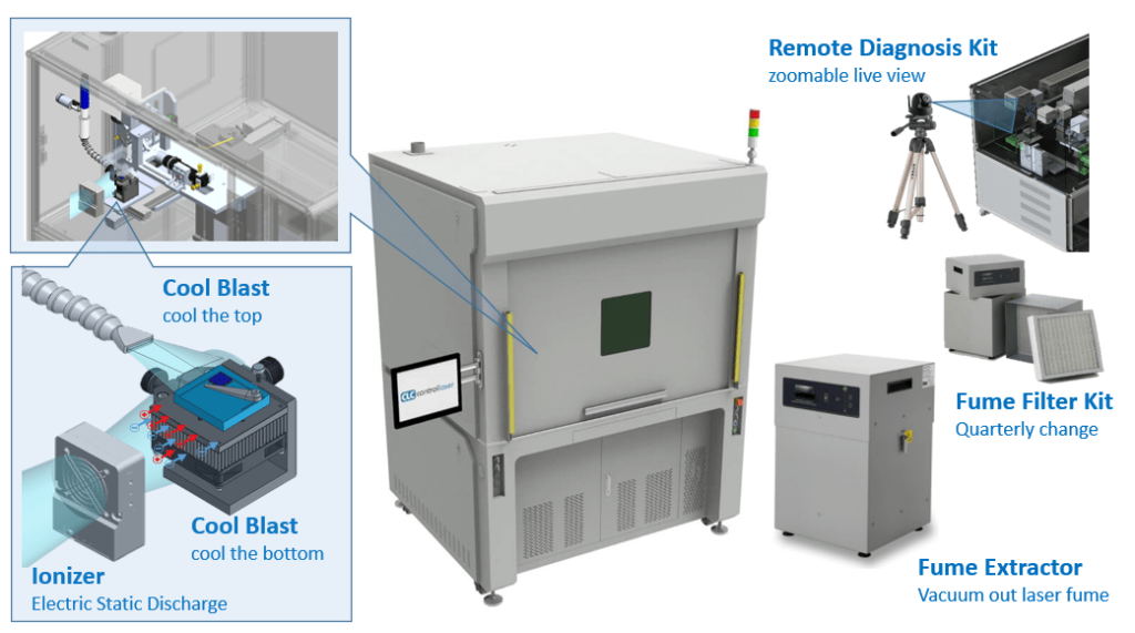
Options: Ancillary Devices
Quotation:
Samples Shipping Address
8251 Presidents Drive, STE 1688
Orlando, FL, 32809 USA
Tel: +1 407 926 3500
Email: [email protected]
Attn: CLC Application Lab
Buyer:
Seller: Control Laser Corporation
Address: 8251 Presidents Drive, STE1688, Orlando FL 32809
Email: [email protected]
Phone: +1 407 926 3500
Payment Terms: 50% Deposit, 50% before Ship
INCOTERMS: ExW
Shipping Date: 6~8 weeks from PO confirmed date
Acceptace Test and Inspection before shipment:
Location: Onsite inspection at CLC’s facility; or Remote inspection by QC report/Video call
Criteria: by CLC’s Outgoing QC Testing Acceptance Critera; or by pre-sale sampling Acceptance Test Critera
By signature and date below, I hereby certify that the above Specification of Supply, Acceptance Test Criteria are well communicated and mutual accepted, and aware of any further changes or additions may come to add-on quote and extra charges, the delay of deposit payments, providing samples and/or fixtures may cause the production and delivery schedule change or order cancellation.
Your personal data will be used to process your order, support your experience throughout this website, and for other purposes described in our privacy policy.